Could you briefly tell us what you are currently working on and how you research field can be described in a few words?
Essentially, we’re building a high-speed camera for the nanoworld. With electron microscopes, we don’t just want to visualize the tiniest structures. We want to track how minuscule components, like transistors, switch during operation; in other words, we’re aiming to look inside a working computer chip in real time. These insights help us not only to better understand today’s technologies but also open up pathways to the components of tomorrow: from more powerful semiconductors and novel optoelectronic elements to magnetic memory devices for spintronics.
Imagine you had to explain electron microscopy and its application to someone without expertise. What would you say?
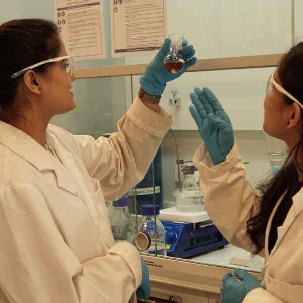
An electron microscope is, in principle, like an extremely powerful magnifying glass, but instead of using light, it uses electrons. This allows us to visualize structures a thousand times smaller than what a conventional light microscope can reveal, down to individual atoms. Electron microscopy is used to investigate materials in all their detail: for example, in medicine to view cells and viruses; in materials science to develop new substances; or in semiconductor engineering to analyze computer chips at the nanoscale. It’s truly a key tool for making the invisible visible.
What is the biggest current challenge of your research project?
The biggest current challenge is to capture ultra-fast processes in the nanosecond range while preparing samples that remain stable under real-world operating conditions in the electron microscope. Preparing such electrically contacted and electron-transparent samples is extremely delicate; critical properties are often lost in the process. To overcome this problem, we developed a special carrier chip system called the FLASHgrid, which significantly simplifies both the fabrication and contacting of these samples. This provides a foundation for conducting reliable experiments on functioning nanoscale devices.
You have also developed the method “Interference Gating”. What makes this method special – and what progress does it represent in comparison to previous techniques?
With Interference Gating (iGate), we have developed a method that makes ultrafast processes directly visible inside the electron microscope, essentially a strobe light for the nanoworld. You can think of it like an entirely new shutter mechanism, similar to a film camera, but with no mechanical aperture needing to close and no film that has to move. This makes the method surprisingly easy to implement, without long downtimes or costly microscope modifications. As a result, we can now capture not only snapshots in the nanosecond range but also entire “movie sequences” of dynamic events, such as the switching of a nanostructured diode.
You are currently developing a product based on your research findings. Could you tell us a bit more about your development?
The FLASHgrid is a MEMS-based carrier chip system that has now reached product maturity thanks to a collaboration with Ferdinand-Braun-Institut gGmbH, Leibniz-Institut für Höchstfrequenztechnik (FBH). It solves a core problem in electron microscopy: until now, preparing tiny, electrically contacted samples was extremely time-consuming and expensive, sometimes taking days for just a single sample. Our chip reduces this effort to just a few hours, as its adaptive electrodes can flexibly adjust to different geometries. This not only makes sample preparation faster and more cost-effective, but also more reliable and reproducible. In the long term, the FLASHgrid enables entirely new workflows in both research and industry. It’s a tool that not only simplifies everyday lab work but also accelerates the development of future nanotechnologies.
What is innovative about it – and who could benefit the most from it, for example in industry or society?
The innovative aspect of the FLASHgrid is that it drastically lowers the barrier of sample preparation. Previously, creating electrically contacted samples for electron microscopy was an expensive, specialized process mastered by only a few experts. Our chip radically simplifies this step: thanks to the adaptive electrodes, a wide range of sample geometries can be quickly and reliably contacted – whether they are semiconductors, optoelectronic structures, or magnetic materials.
This benefits research labs, which can significantly increase their throughput, as well as the industry, particularly in semiconductor and materials development, where time is literally money. The FLASHgrid enables shorter development cycles while offering deeper insights into next-generation components. It is, therefore, both a driver of innovation in basic research and a tool with direct added value for tomorrow’s technologies.
Flashchip Prototyp
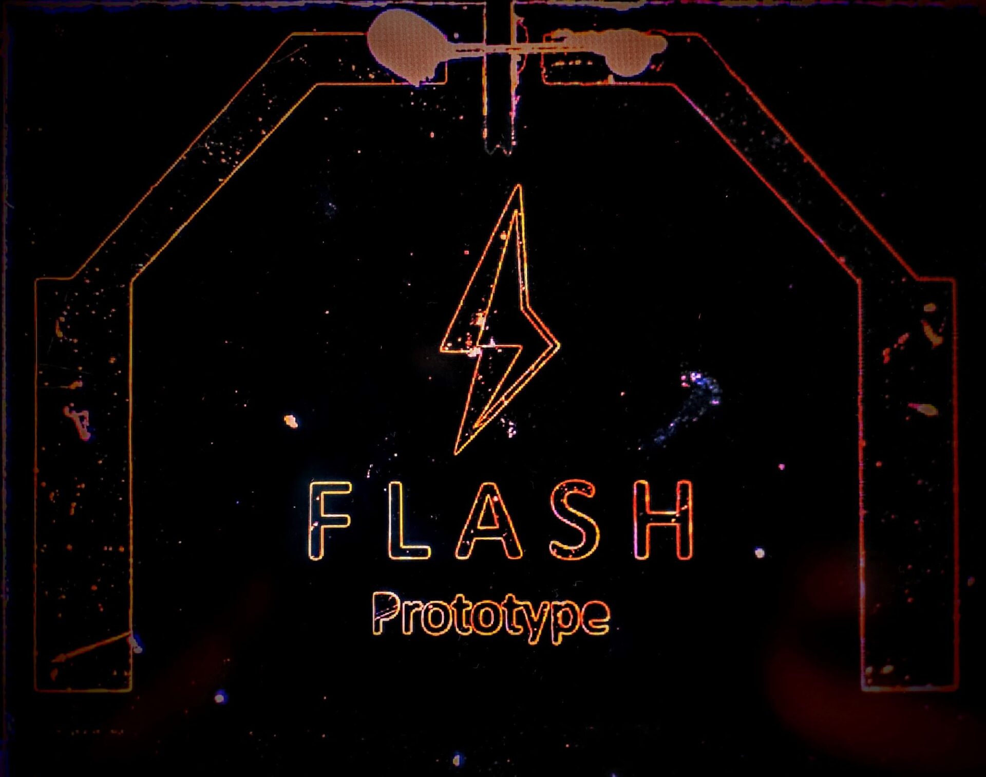
Prototyp Flashchip
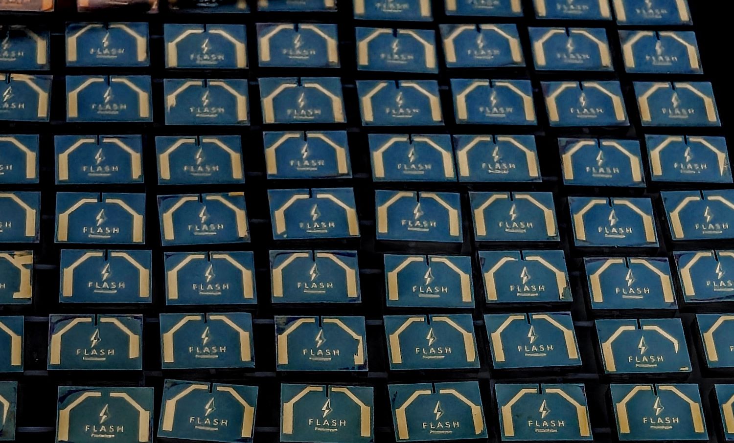
Prototypes of the FLASHgrid
Beyong its current applications: Which other possibilites do you see for how your research could influence our lives in the future?
What fascinates me most about my work is that with our methods, we don’t just gain a better understanding of existing materials – we are also laying the groundwork for future technologies. When we learn how electrons move in nanostructures and how components actually function during operation, we can develop more powerful and energy-efficient chips in the future. But the perspectives go far beyond that: our methods also allow for the investigation of novel optoelectronic systems, such as for quantum communication, or magnetic structures for spintronics. In the long term, such insights could even help develop more sustainable materials or form the basis for entirely new computing and memory technologies. In this sense, I see electron microscopy not just as a tool for analysis, but as a key to unlocking future technological leaps.
Which industries or companies could benefit from a collaboration with you?
The most obvious application is in the semiconductor industry, which is constantly working on developing smaller, faster, and more energy-efficient components. Here, our methods can directly help to better understand how new structures function and to shorten development cycles. Companies in optoelectronics – for instance, for next-generation LEDs or photonic devices as well as the magnetics and spintronics sectors, which are working on future memory and computing architectures, also stand to benefit.
Beyond that, research institutes and companies in materials development are potential partners: anyone researching new materials for sustainable technologies, batteries, or quantum applications gains a crucial advantage from high-resolution, time-resolved insights. With the new DElPhIN lab we are currently building at the Institute of Physics at Humboldt University Berlin, we are laying the foundation for exactly this: a specialized laboratory for dynamic electron phase imaging, enabling close collaboration between university research and industry.
What originally motivated you to choose this field of research?
From the beginning, it was never just the application of a method that fascinated me, but its further development. Even during my studies, I was drawn to tinkering with the instruments themselves and exploring how to expand their capabilities – a red thread that has run through my bachelor’s, master’s, and PhD. I’ve always been driven by the belief that with new tools, you can also ask and answer new questions.
What moves me deeply is that I get to continue this work in Berlin, the city where not only the electron microscope was invented, but also the foundations for time-resolved electron microscopy were laid. Being able to develop my own innovative methods in this field is a great honor and also a very personal motivation. Because what drives me is not so much the idea of creating something entirely new for myself, but rather making a contribution that enables future generations of researchers to gain new insights into the world of the smallest structures using improved instruments.
Was there a pivotal moment in your career that particularly shaped your passion for science?
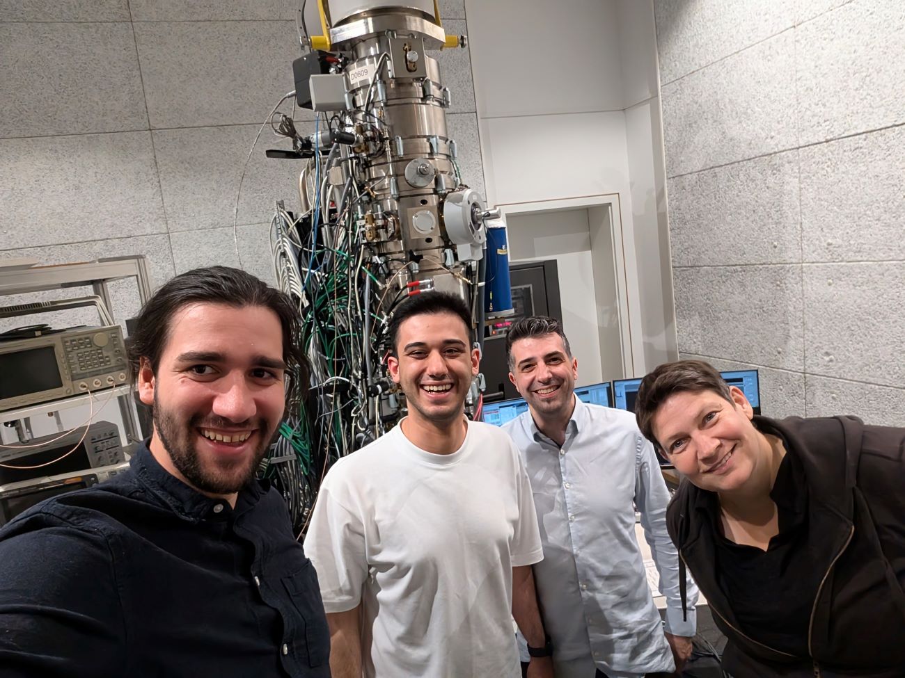
There wasn’t one single pivotal moment for me, but rather many small ones that came together over the years. Scientifically, a key moment was certainly when we first broke the nanosecond barrier with iGate and were able to directly visualize charge transport in a switching semiconductor. But just as influential were the encounters with people whose contributions to electron microscopy have changed our view of the world. Awards and recognitions for my research have also shown me that I’m on the right track, a nice feeling that motivates me to keep going. But the most important thing for me has been finding fellow travelers along the way: long-time colleagues who have become friends. Without that team spirit, the many long nights in the lab would have been nearly impossible.
What personally fascinates you the most about your work today?
What fascinates me most today is that we’re developing tools that not only enable new insights into physics, but also make daily lab work easier for many. A great example is the FLASHgrid: it makes the labor-intensive and expensive preparation for electrically contacted experiments significantly faster and easier. It’s important to me that this doesn’t just benefit us, but also frees up researchers around the world, allowing them to focus more on the scientific questions themselves rather than getting lost in long preparations. Seeing that a tool we developed from an idea is now tangibly contributing to more efficient and accessible research is one of my biggest motivations.
Research can be frustrating sometimes. How do you deal with setbacks?
Setbacks are just part of research; sometimes, despite months of preparation, an experiment fails due to a detail that couldn’t have been foreseen. I try to see this as a learning process: every failure shows me where to look more closely and often opens up new ideas I hadn’t considered before. The team is also crucial: when you’re pulling all-nighters together in the lab, you share both the disappointments and the small successes. That makes setbacks more bearable and ensures that something positive always comes out of them in the end.
If you could make one wish, what would be the first research question you’d want to answer?
If I could wish for one thing, it would be an answer to how far we can push time-resolved electron holography. We recently broke through the picosecond barrier, a huge step that showed what’s possible. At the same time, we’re already working on an optoelectronic implementation that could even take us into the femtosecond range. This would create a tool that allows us to make the three-dimensional potential distribution of fundamental physical processes visible like a film, to literally film electrons at work. For me, that’s a fascinating vision: that in the future, we won’t just understand what happens, but actually witness how it happens.
And finally: Is there something that often surprises people when they meet you outside the lab?
When I do manage to stop thinking about physics, I devote myself to my many hobbies, which also often involve working with my hands: from turntablism, to tinkering with cars, to building movie prop replicas. I also try to spend as much time as possible with my family. A great compromise that brings a lot of these things together, for me, are science slams. We usually all have a great time there and I only talk about my work for ten minutes.